Wafer-wafer bonded semiconductor detectors
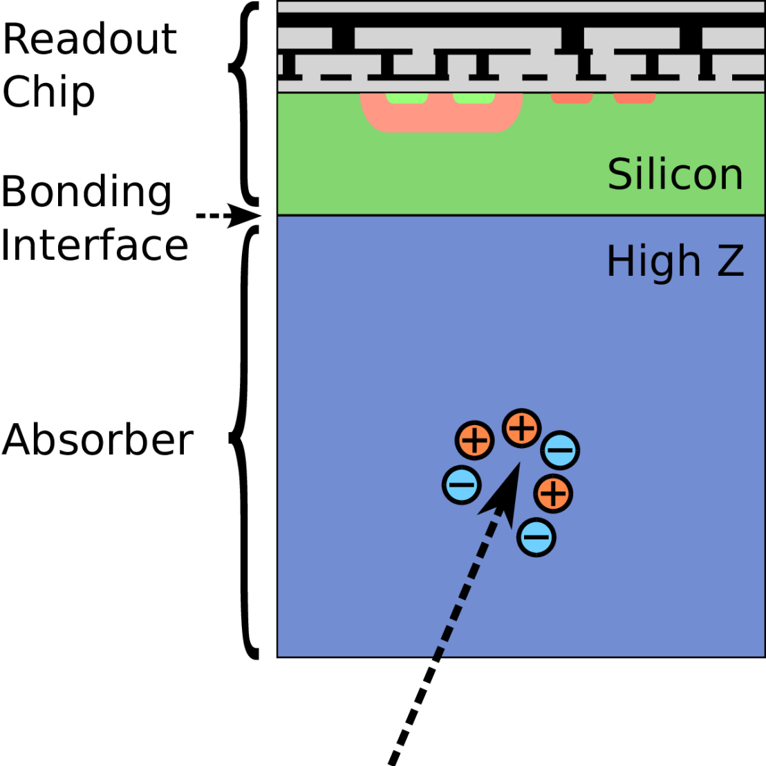
For building X-ray pixel detectors the use of High-Z absorber materials (such as GaAs, CdTe SiGe etc.) is beneficial, as these materials offer a much higher interaction probability compared to silicon. The higher interaction probability enables the fabrication of highly efficient sensors. In the context of medical X-ray imaging this would allow to reduce the radiation dose a patient is exposed to.
We are investigating the use of low-temperature wafer-wafer bonding (surface activated bonding) for the assembly of such detectors, as an alternative to the hybrid and monolithic approaches for fabricating pixel sensors. Under this approach, a fully processed CMOS wafer (containing the pixel readout chips) is covalently bonded to a (potential High-Z) absorber wafer (which forms the active P/N junction). Current investigations focus on a precise characterization of the resulting bonding interface and its influence on the signals generated in bonded detectors. For this investigation pad diodes have been fabricated in-house by bonding high resistivity float-zone silicon wafers.
Our investigations are based on various measurement techniques, including transient-current-technique (TCT), current-voltage (I/V), energy-dispersive X- ray spectroscopy and other measurements. The results of these measurements are compared to and complemented by simulation results based on Synopsys Sentaurus TCAD, custom Python-based simulations and other simulation tools.
Current work is focusing on refining and generalizing initial results. Future inves- tigations will focus on the application of this technology on pixelized detectors, as well as the practical integration of High-Z sensor materials (e.g. GaAs, CdTe or similar).